UV pcb exposure box

Today, I want to write a few words about another of my older projects.
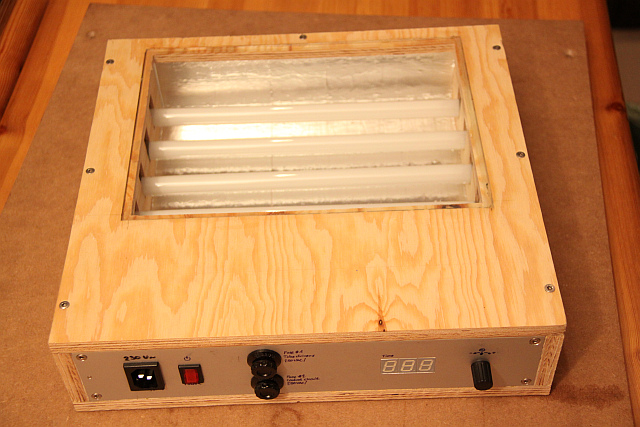
UV exposure box - whole view

A while ago, I started building this DIY UV exposure box. The electrical part consists of a self-designed count-down timer based on an AVR Tiny2313 CPU, 4x8W PHILIPS UV tubes, ignition/driver circuits from cheap fluorescent bulbs, a multiplexed numeric LED display, a rotary encoder and some wiring. A piece of ~4mm aluminum serves as a faceplate, picture frame glass as the exposure surface. We’ll have a look inside in a moment.

When turned on, the controller presents the configuration menu first. All options are preset – or should I say ‘preprogrammed’ because the preset cannot be changed, as of yet – to the values I use most frequently. Configuration includes the time (up to 9min 59sec), a variable tube preheat time up to 59 seconds and a zone selection. The zone selection does nothing at the moment, but the pcb features a mounting spot for a second solid state relais which I have not yet installed. Which means, all four tubes are activated.

Exposure box - menu
Minutes…

Exposure box - menu
Seconds…

Exposure box - menu
Zones…

Exposure box - menu
Preheat…

Exposure box - menu
…ready to go!

Exposure device - running
Enjoy

Press the selector one more time and the process starts. To stop again, either press the button again, switch off the mains or wait patiently until the time runs out.

Now, on to the inner values. After undoing 7 torx screws, the lid can be removed to access the elecronics compartment behind the front panel:

Exposure device - mains part
Mains input and ignitors

Exposure device - microcontroller
Microcontroller board

Exposure device - electronics compartment
Electronics compartment

Inside the compartment is the four-fold ballast circuit, which consists of four board found in the sockets of fluorescent energy saving lights. These are pretty cheap compared to commercial electronic or inductive ballasts and they can be used right as they come. The only crucial number is the power rating – my tubes are rated for 8W while the ballasts came from 9W bulbs, which works just fine. Care has to be taken when opening the sockets, though. The bulbs should be left lying around for some time prior to “dissection” because they contain a pretty juicy capacitor. The circuit inside is basically a simple switchmode current supply. When that’s done, an easy way is to cut them open along the circumfence about in the middle of the socket’s height with a fine saw blade. Don’t cut too deep or you will damage the pcb. Once the casing is open, mark the pairs of wires coming from each end of the tube before cutting them. These pairs need to go to the ends of the UV tube, don’t mix them up or you’ll short out the circuit. How the two wires connect to the two pins of the tube on each side is completely up to your choice, though.

As always, remember the hazards involved when dealing with mains equipment, especially such that was never designed to be opened or even run in the open. Also, don’t go breaking any fluorescent tubes as they might contain traces of mercury.

The four ballasts are wired in parallel to the mains, with just a fuse, the power switch and a solid state relais in series. Fuse-wiring got a little complicated because I forgot to place separate fuse sockets for controller and drivers onto the pcb, but nothing dangerous here. A connection between faceplate and protective earth is also present for safety reasons, seeing that there is lots of live wiring very near. You may have noticed the absence of any cooling fan or holes – these are not necessary as the device is run for a few minutes at a time and never unobserved. The ballast circuits are designed for operation in a very tight unventilated space anyways, so no trouble to that end. After ~5 minutes of exposure the glass surface becomes just noticeably warm.

To the right is the control circuit, consisting of said ATTiny2313, a small 6VA transformer-powered 5V supply, the solid state relais (SHARP S202S02) and three npn transistors as segment drivers for the LED display. I still have some pictures from back when I made the pcb (about a year ago now):

Drilling holes…

Finished pcb

…all soldered.

I have used this exposure box several times now and am pretty content with the results. There still remains some creepage of light between the layout print and the photosensitive layer, resulting in fuzzy edges of traces and larger groundplanes sprinkled with small holes. This is partly thanks to an absolutely ridiculous laser printer made by HP (Color LaserJet 2600nse). No matter what settings are used (even in the expert options), the printer will never do dense black withing planes and very often blur traces on either the leading or trailing edge. Text works fine, though.

You may download the schematics in Eagle 6 format at your leisure. I do not guarantee correctness of the layout, though. There was a small problem in an earlier version (Pin 1 of ribbon cable connector was not connected to ground) which I have fixed now.

I do not take any responsibility for whatever happens to you. It’s up to you to decide if you want to and are able to build something like this.

>> EAGLE 6.0.0 Schematic and Layout

>> Script files for older versions of EAGLE – untested!

>> Sourcecode and .hex for ATTiny2313

* NOTE: Make sure that pin 1 of the front panel connector is really connected to ground, the traces were etched away in my case. The result is erratic behaviour of the rotary encoder.

Minor setback

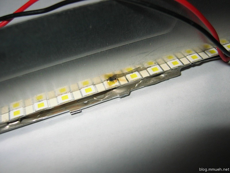
Somehow I knew that this went over too easy. Fortunately, magic smoke SMELLS. Just got the battery out in time, but part of the damage already happened.

Defective LED
Bang!

Defective LED
...and another.

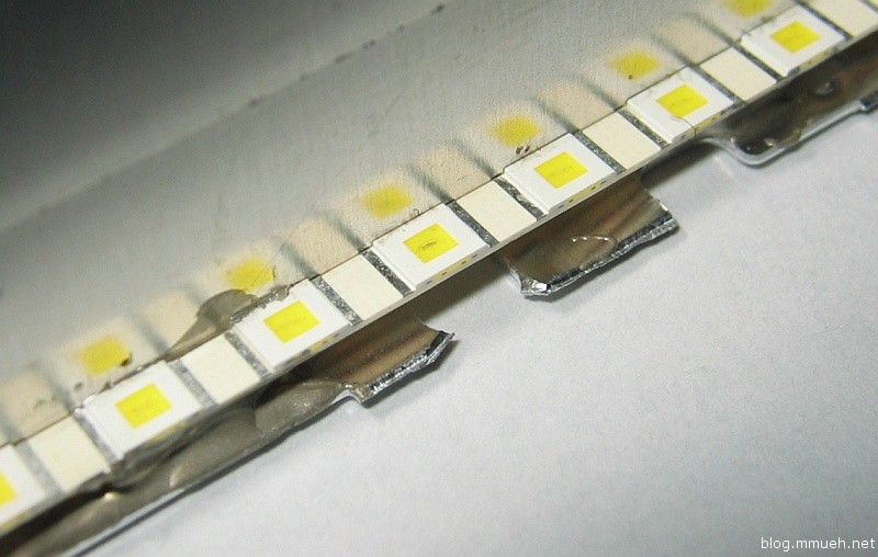
Some days ago, one of the triple-chains on the right half of the screen went out. While the darker area is clearly visible, the shadow is still illuminated by the neighboring LEDs. The cause is the LED in the second picture, the damage is only visible as a slight dark streak in the center of the yellow part. Then today the backlight fuse blew out of this world, and the reason is seen in the first picture. I knew this was a close call, but precisely “calibrating” the almost not existent isolation gap between LEDs and metal (by wedging a piece of paper in every here and there during glueing :-D ) gave me no no reason for concern. Maybe some flexing or thermal deformation did the rest.

Anyhow, got to rebuild this part. Not too bad though, the stripes are inexpensive and I wanted to include a diffusor sheet anyway. As good a chance as any I guess.

Edit: By the way, the driver circuit survived the whole mess just fine. That IC is some tough design! Haven’t managed to fry a single one of those so far.

DIY LED TFT Backlight

Today I finally got around to finishing my first design for a switching  LED display backlight driver. The circuit is built around a LT3518 switch mode driver IC working in buck (step down) mode in this application.

LED driver pcb topside

LED driver pcb bottom

Someone figure out why SMD hand-soldering always looks ugly on macro images…but trust me on this, the circuit works like a charm ;-) The flux residues don’t hurt performance, but you really do want to keep any solder-balls or whatever metalliccy is floating around your circuit away from the tight parts.  If necessary, rinsing it with alcohol while carefully assisting with a brush does the job, followed by a soft coating of plastic spray to prolong the circuit’s life.

My design was done rather quick and dirty because it needed to get done. Just don’t expect THE most absolutely high frequency capable layout, though I guess that prominent airwire in the first picture crashes this illusion anyways. Consider this more of a first prototype to check out what this chip has up its sleeve in buck mode after already trying boost mode on Tobi’s LED driver, which will also be documented later on. So far, it seems to keep up with my demands quite well, it will be modified and optimized later on.

Measurements (all taken at maximum brightness with a tRMS multimeter):

V in I in V out I out P in P out Efficiency
Mains 20 V 0.25 A 9.6 V 0.400 A 5.0 W 3.84 W 77 %
Battery 11 V 0.41 A 9.6 V 0.400 A 4.51 W 3.84 W 85 %

Higher efficiency on battery is just perfect, even though it is barely into the operating voltage range. The measurements made on the go, so the numbers might not be absolutely accurate. If there is time, the scope will clear that up. Also, keep in mind that battery voltage will drop some over time. According to standard Li-Ion specs, it ranges from 12.75 V charged to 9.3 V discharged (although I have never seen it go below 10.5 V so far).

The schematic and board layout will be available in the next few days in EAGLE format, together with more photos of the “implanted” driver. Need to clean up the parts naming and stuff first.

While I am on it, enjoy my wicked hand drawing skills :-D

Prelim. schematic
Prelim. schematic

Layout description
Layout description

A few things to add to the drawings: First, the schottky-diode is of SK34A type, secondly the ceramics are all of X7R-rating type (refer to datasheet of  the LT on this one) and thirdly the connection between TGEN and CTRL/VREF ist also an airwire, which can clearly be seen dominating the circuit in the pictures and is unbelievably oversized.

This article will be followed by some pictures of the LED array and driver mounted inside the display. The former was already installed before I started this blog so I didn’t think of taking some shots at the time. It is nothing spectacular really, some chip-on-board (COB) slimline LED modules bought over at led-tech.de, soldered together and cut to correct length, then glued into place instead of the CCFL with thermal conductive glue.

NOTE: While testing the device to its limits, I am experiencing some problems at very low system voltage. When on battery only, the notebook’s internal supply lines drop to around 10 to 12 volts as opposed to rock-solid 20V when the mains is connected.

This driver was designed with up to 20V and only down to about 12V input in mind, which means a maximum of 80% switching duty cycle at low voltage. I figured that the internal supply lines would be thoroughly regulated but was mistaken as it seems. As soon as the voltage drops a quantum too far while powered only by batteries (eg. more power is drawn by any device), duty cycle rises over some magic number around 96% at 250kHz (see data sheet) and flickering occurs as the IC loses control over the current. This is why there certainly will be a v2 of this, and it will be buck-boost-mode to handle low voltage situations even better. I might also want to fix minor problems with shutdown mode still allowing a very small current through the ICs internal switch, but in comparison this one is totally unimportant.

Right now the v1 driver is successfully implanted in the screen bezel and works nicely. Screen brightness even beats the original CCFL backlight, though the lower screen border is not absolutely uniformly lit. I could care less, thanks to the windows taskbar using up that space. The notebook is a SX65S by the way.