Yes, this is about fancy displays – again. I have been wondering for a while whether it could be simple to repurpose the LED matrix displays often found in Jura coffee machines. Mounted behind tinted plastic they give the front panel a distinctly premium look. Coincidentally, they look highly similar to the Osram- and Avago-made PDSP/HDSP intelligent dot-matrix module series, which is what I was initially expecting to find when pulling apart the control panel of a scrapped Jura Impressa C9. Let’s just say the expectation was pretty far from the mark.
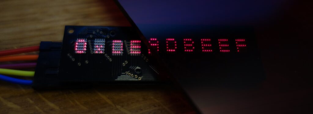
What is actually being used is somewhat of a curiosity. Instead of embedding commercial modules, Jura seems to have chosen the high road by having a custom module fabricated. In this case it is a 10-character module, consisting of 5×5 red LED pixels per character. This module consists of a stack of two PCBs – other variants may also exist, depending on machine type – to one of which a matrix of discrete LED dies is bonded openly. Not only does this make the module rather exciting to handle (note to self: try not to touch or sneeze at bond wires), but it also has me wondering about the controller and its capabilities.
HDSP-/PDSP-series displays come equipped with an integrated charset controller, which has all commonly used characters stored in an integrated ROM. Characters – usually 5×7 pixels – are recalled by writing the corresponding index into the module RAM, which is done via either a parallel or serial bus. Afterwards, the display begins printing the selected letters by applying a clock, which has the display controller scanning the LED matrix either line-, column-, or pixel-wise, depending on the module type. Pretty simple, huh?
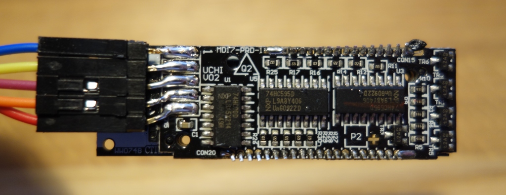

The Jura module, it appears, does not have an integrated controller at all, although control circuitry is embedded. Upon close inspection, six ICs can be seen on the piggy-back PCB shown in Fig. 1. Three on the visible backside are one 74HC00D quad-NAND and two 74HC595D shift-registers (SRs). Since there are a lot of pixels to control, this makes me suspect that the three inaccessible chips sandwiched within are also 595s, and that all five SRs are connected in a daisy-chain to allow data to be shifted from one to the other. The HC00 is then probably either used as a signal inverter or as a buffer. Externally, the module is connected by five wires: two are easily validated to be GND (1) and +5V VCC (5) by probing the exposed IC power pins, and one can be traced to the SR shift clock (3). That leaves two pins for latching (4) and for the data signal (2), which run through (or by) two of the NANDs. All in all, the bare minimum required to operate a shift register chain and therefore a clear sign for this display to neither have a character ROM, nor any special features such as dimming control – unless channels of one of the registers are used as a current-setting DAC.
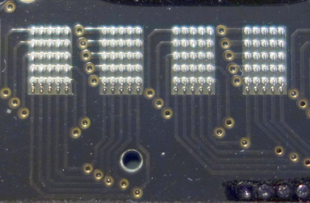
What is very unclear at this point is how the matrix is supposed to be addressed. Each 595 has one byte of storage, equalling eight outputs, and five registers thus make up forty channels. A number of SMD transistors on the control PCB suggest that some channels are being amplified, probably as block drivers, and by inspecting the matrix grid on the front PCB (compare Fig. 2) it appears as if two neighboring characters share the same column drive but do not share lines. Let’s start with the assumption of 5 individual blocks, each operating at 5 columns and 10 rows. That makes every pixel individually adressable, requiring a total of 20 adressing lines. Seeing that 20 data lines are left and that such a configuration requires some kind of logic overhead to entangle the block-drive and column-drive signals – usually done on the cathode side – it could well be possible, that 5 individual column lines are running to each two-char block instead of using block enable signals. This brings us to 10+25=35 control lines. The extra 5 are probably either left unused, or otherwise utilized for e.g. brightness control.
Let’s check this assumption by using an Arduino Nano clone to drive the three data lines. The sequence is simple: apply data bit, clock high. Next bit, clock high. Repeat 40 times until the bit-chain has propagated through all registers. Then drive the latch pin high to move all data into the output registers. Of course writing all ones is likely to wreak total havoc, which is why I tend to start with few set bits. Since LED displays are designed for scanning and not for continuous display, there is a chance that LED chips may be damaged by continuous illumination. I am therefore writing a chain of zeroes immediately after each data word, and controlling the duty cycle such that the display is only supposed to flash for ca. 50 milliseconds per second. The data words consist of different patterns: three ones, distributed equally with 15 zeros distance to maximize the probability of hitting a row and column drive at the same time, a single one at the beginning and a series of 8 ones at the end, and finally a single one on the end with 8 ones at the beginning. By my definition, the “end” of the word (bit 39) is what is transmitted last.

These words are then shifted through the display buffer cyclically, leading to different patterns of the LED matrix. From the patterns, I can deduce that the row drives must be at the end of the data word (or in the first register), while the columns must be nearer to the beginning of the word. However, there is some interleaving of characters going on as the sequence of columns appears a bit erratic.
I therefore start to flash individual bits, which confirms the location of the row and colum signals. The registers are mapped as follows:
| Bit | 7 | 6 | 5 | 4 | 3 | 2 | 1 | 0 |
| 39-32 | row_B5 | row_B4 | row_B3 | row_B2 | row_B1 | row_A5 | row_A4 | row_A3 |
| 31-24 | row_A2 | row_A1 | col_5_5 | col_5_4 | col_5_3 | col_5_2 | col_5_1 | col_3_5 |
| 23-16 | col_3_4 | col_3_3 | col_3_2 | col_3_1 | col_9_5 | col_9_4 | col_9_3 | col_9_2 |
| 15-8 | col_9_1 | col_7_5 | col_7_4 | col_7_3 | col_7_2 | col_7_1 | col_1_5 | col_1_4 |
| 7-0 | col_1_3 | col_1_2 | col_1_1 | n/a | n/a | n/a | n/a | n/a |
row_AX/row_BX means “character A (odd-numbered) or B (even-numbered) in active pair, row X”.
col_Y_Z means “column drive for character Y (odd), column Z, and character Y+1 (even), column 5-Z”. Characters are numbered 1 through 10 beginning with the one closest to the connector. Columns are numbered 1 through 5 left-to-right, and rows 1 through 5 top-to-bottom.
It appears that my assumption is spot-on. Linked columns in neighboring characters are reversed in order, which I could have seen from the layout but did not pay attention to. Also, I could not find any functionality in the lowest bits (marked n/a), which means that my assumption about them being left out is probably also correct.
To achieve the maximum transfer speed, two columns can be written at once, although this puts quite a bit of load on the column drivers if both columns are illuminated. Thus, twenty-five consecutive writes of the entire chain are necessary to display the total of 50×5 pixels. For an adequate display persistence, this procedure must be repeated at least 30 times per second, yielding a pixel clock rate of ca. 30 kHz. No big deal for state-of-the-art microcontrollers, but still a problem if the CPU is supposed to handle more important jobs, too. This display type therefore requires a dedicated microcontroller – albeit a tiny one – or else, a controller possessing a DMA module capable of sending the bitstream from memory without producing CPU load.
uint8_t juraBuffer[50];
uint8_t juraSendBuffer[5];

...

inline void juraSendHi( void ) {
  // Apply high, then clock once.
  PORTD |= (1<<PIN_DATA);

  PORTD |= (1<<PIN_CLK);
  PORTD &= ~(1<<PIN_CLK);
}

inline void juraSendLo ( void ) {
  // Apply low, then clock once
  PORTD &= ~(1<<PIN_DATA);

  PORTD |= (1<<PIN_CLK);
  PORTD &= ~(1<<PIN_CLK);
}

inline void juraLatch ( void ) {
  // Drive the latch high
  PORTD |= (1<<PIN_LAT);
  PORTD &= ~(1<<PIN_LAT);
}

inline void juraEncode2c( uint8_t buf[5], uint8_t block, uint8_t col ) {
  // Encode a pair of columns for transfer to the display
  // Correct order of blocks:
  // 1+2, 9+10, 7+8, 3+4, 5+6
  // Achieved by switching bit 1 and 2 of block number (in range 1...5)
  uint8_t tblk = block;
  if (tblk > 3) tblk = tblk - 2;
  else if (tblk > 1) tblk = tblk + 2;

  uint8_t tv = tblk * 5 + (col - 1);
  uint8_t bynum = tv >> 3; // Divide by eight
  uint8_t binum = tv - (bynum << 3);

  buf[0] = 0;
  buf[1] = 0;
  buf[2] = 0;
  buf[3] = 0;
  buf[4] = 0;

  buf[bynum] |= (1<<binum);

  // Decode, which buffer column goes where. Use only the low 5 bit of buffer bytes.
  uint8_t X = (block - 1) * 10 + (col - 1);
  uint8_t Y = (block - 1) * 10 + 10 - col;
  buf[3] |= (0xC0 & (juraBuffer[X] << 6));
  buf[4] |= (0x07 & (juraBuffer[X] >> 2)) | (0xF8 & (juraBuffer[Y] << 3)) ;
}

inline void juraXferBuffer( void ) {
  uint8_t temp;

  for (uint8_t i = 0; i < 5; i++) {
    temp = juraSendBuffer[i];

    for (uint8_t k = 0; k < 8; k++) {
        if ((temp & 0x01) == 0)
          juraSendLo();
        else
          juraSendHi();

        temp >>= 1;
    }
  }
  juraLatch();
}

void juraUpdateDisplay( void ) {
  uint8_t temp;

  for (uint8_t i = 1; i <= 5; i++) {
    for (uint8_t k = 1; k <= 5; k++) {
      juraEncode2c(&juraSendBuffer[0], i, k);
      juraXferBuffer();
    }
  }
}
Download the full code here: juraled.ino
I wrote this set of routines to display the contents of a display buffer on the screen. Admittedly, there is a bit of memory overhead as the buffer carries 8-bit columns where only 5 bits are required. The transmission routine then selects the correct columns from the buffer and transfers them, two at a time, into the shift register. What I have not yet figured out completely is how to increase the brightness. Obviously, the display needs a tinted window to improve its contrast, but that is not all. One possibility is to drive single columns instead of pairs, which requires more write cycles per update but reduces the burden on the column drivers.
Any chance you have this display still? I’m trying to replace the broken one on my E8. I can’t find one anywhere and I think it’s the same as this one. If you aren’t using it for a project or something I’d be happy to buy it off of you.
Hi, Mario!
Thank you for your work!
Can you show complete working Arduino example code?
Sure, grab it at https://blog.muwave.de/download/juraled.ino!
In this version the text is hard-coded, so you might need to add an extra routine to translate text into charset.
Thanks!